Unlocking Success: The Advantages of Advanced PCB Fabrication Techniques for Global Buyers
In the evolving landscape of electronics, the significance of advanced PCB fabrication techniques cannot be overstated. According to a report by MarketsandMarkets, the global PCB market is projected to reach $90.7 billion by 2025, driven by the increasing demand for sophisticated electronic devices. As the complexity of electronic designs grows, so too does the necessity for high-precision PCB fabrication methods that can accommodate intricate layouts and enhance reliability. These advanced techniques not only improve manufacturing efficiency but also contribute to cost savings and product performance, which are crucial for global buyers seeking to stay competitive in a fast-paced industry. By understanding the benefits of these innovations in PCB fabrication, companies can unlock substantial advantages, ultimately leading to increased market share and customer satisfaction.
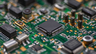
Benefits of Advanced PCB Fabrication Techniques for Global Buyers
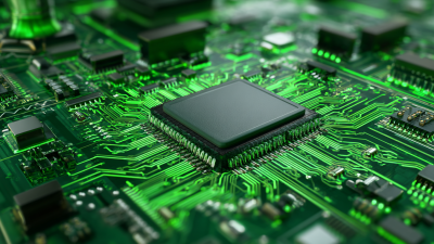
As the electronics industry continues to evolve, advanced PCB fabrication techniques are becoming vital for global buyers looking to stay competitive. These techniques, such as automated processes, high-density interconnects (HDI), and the use of flexible materials, enhance the overall performance and reliability of printed circuit boards. By investing in advanced fabrication, manufacturers can produce more complex designs that allow for greater functionality within smaller footprints, catering to the increasing demands of modern technology.
Moreover, advanced PCB fabrication techniques offer significant cost efficiencies and reduced time to market. Streamlined processes and innovative manufacturing solutions minimize waste and enhance productivity, translating to lower production costs for global buyers. Additionally, these techniques allow for rapid prototyping and faster iteration cycles, enabling companies to respond swiftly to market demands and technological advancements.
With the ability to deliver high-quality, customized solutions, global buyers can achieve a competitive edge and improve their overall product offerings in an increasingly dynamic marketplace.
Key Factors to Consider When Selecting PCB Fabrication Partners
When choosing a PCB fabrication partner, several key factors come into play to ensure successful collaboration and high-quality output. First and foremost, expertise in advanced fabrication techniques is essential. Partners who are well-versed in state-of-the-art technologies not only deliver superior products but also adapt to the rapidly evolving demands of the electronic market. Buyers should look for partners that have a proven track record in handling complex designs and a variety of materials while maintaining strict quality control standards.
Another critical factor is communication and customer service. Global buyers need partners that are responsive and proactive in their communication, providing updates throughout the fabrication process. A partner with a strong support team can swiftly address any issues that arise, minimizing downtime and delays. Additionally, geographical location can also influence shipping time and costs, making it essential for buyers to consider logistics when selecting a fabrication partner. By carefully evaluating these factors, buyers can ensure they choose a reliable PCB fabrication partner that meets both their technical and operational needs.
Unlocking Success: Advantages of Advanced PCB Fabrication Techniques
This bar chart illustrates the key advantages of advanced PCB fabrication techniques as perceived by global buyers. Each advantage is measured on a scale of 0 to 100, showcasing their importance in the selection of PCB fabrication partners.
Essential Checklist for Evaluating PCB Manufacturing Capabilities
When selecting a PCB manufacturer, evaluating their capabilities is crucial to ensure your project's success. An essential checklist should include a review of the manufacturer's certifications and quality management systems. Look for industry certifications such as ISO 9001 or IPC standards, which demonstrate their commitment to maintaining high-quality production processes. This not only reassures you about the reliability of the PCBs but also ensures compliance with global standards, which is critical for market competitiveness.

Another key aspect to investigate is the technology and equipment used in the fabrication process. Advanced PCB fabrication techniques, such as HDI and multilayer capabilities, can significantly enhance the performance and reliability of your products. Evaluate the manufacturer's machinery, including the types of materials they use and their ability to handle complex designs. Additionally, assess their turnaround times and production capabilities to ensure they can meet your scheduling demands without sacrificing quality. A manufacturer who invests in the latest technology is likely to provide you with innovative solutions that meet the evolving needs of the market.
Innovative Trends in PCB Fabrication to Watch in the Market
The landscape of PCB fabrication is undergoing a significant transformation, driven by innovative trends that are reshaping the electronics manufacturing industry. As we look toward 2026, advanced techniques such as 3D-printed electronics are projected to dominate the market, with estimates suggesting a remarkable growth potential in the coming decade. Reports indicate that the 3D electronics market, which integrates additive manufacturing, will play a pivotal role in replacing traditional PCBs with integrated electronics, thereby enhancing design flexibility and reducing production costs.
One notable trend is the increasing adoption of PCB design software, expected to reach a staggering $9.2 billion by 2031. This surge is fueled by rapid advancements in hardware innovation and the demand for AI-powered design automation, allowing manufacturers to create more compact and efficient designs. Additionally, the multilayer printed circuit board market is projected to grow significantly, reaching USD 38.57 billion by 2032, driven by a CAGR of 3.36%.
**Tips:** When evaluating PCB suppliers, prioritize those that embrace cutting-edge technologies to stay competitive. Additionally, consider the long-term benefits of investing in advanced design software, as it can facilitate faster prototype development and enhance production efficiency. Lastly, keeping an eye on the automotive PCB market, which is anticipated to grow substantially by 2035, can provide insights into emerging industry demands.
Unlocking Success: The Advantages of Advanced PCB Fabrication Techniques for Global Buyers - Innovative Trends in PCB Fabrication to Watch in the Market
| Technique |
Advantages |
Market Trend |
Future Outlook |
| HDI (High-Density Interconnector) |
Increased functionality in smaller form factors |
Rising demand in consumer electronics |
Continued growth in mobile devices and wearables |
| Flexible PCBs |
Space-saving and lightweight designs |
Increasing usage in automotive and medical devices |
Expansion in innovative applications like IoT |
| Multilayer PCBs |
Enhanced performance with high route density |
Growing in high-frequency applications |
Expansion in telecommunications and aerospace sectors |
| Embedded Passive Technology |
Reduces component count and improves reliability |
Increasing focus on miniaturization |
Greater integration in compact devices |
| 3D Printed PCBs |
Rapid prototyping and customization |
Innovation in rapid development sectors |
Potential for widespread adoption in creative industries |
Cost-effective Strategies to Enhance PCB Production Efficiency
In today's competitive electronics market, advanced PCB fabrication techniques are essential for global buyers seeking cost-effective strategies to enhance production efficiency. According to a recent report by Research and Markets, the global PCB market is expected to reach $85 billion by 2025, driven by the increasing demand for smaller, more efficient electronic devices. One of the key factors contributing to this growth is the adoption of advanced manufacturing processes such as automation and additive manufacturing, which significantly reduce production time and material waste.
Moreover, advanced techniques such as high-frequency PCB fabrication and microvia technology allow manufacturers to produce more intricate designs with improved performance and reliability. A study from IPC (Association Connecting Electronics Industries) highlights that companies implementing state-of-the-art fabrication methods can achieve up to a 30% reduction in production costs while increasing yield rates by as much as 25%. This not only benefits manufacturers but also appeals to global buyers who are always looking for ways to optimize their supply chain and minimize expenses without sacrificing quality. As the demand for innovation continues to escalate, embracing these advanced PCB fabrication strategies becomes a critical differentiator in the global marketplace.