
What Is the Best Solar Cell Carrier in 2026?
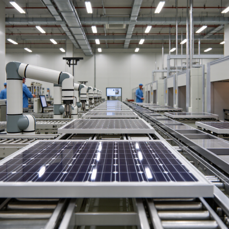
In 2026, choosing the best Solar Cell Carrier is not simply a materials question. In this context, the term means the tray, cassette, or fixture that supports wafers during production. It must protect fragile cells while moving reliably through the factory. A polished specification can look convincing. The production line is the real test.
Market growth makes that choice more consequential. IEA PVPS’s Trends in Photovoltaic Applications 2024 report estimated that global installations reached about 456 GW in 2023. That figure signals scale, not a single preferred carrier design. The 2024 International Technology Roadmap for Photovoltaic (ITRPV) also tracks larger wafer formats and continuing reductions in wafer thickness. Both trends raise practical demands on support, alignment, and handling. Small details matter.
A useful comparison should therefore examine wafer compatibility, thermal and chemical resistance, particle control, loading speed, and breakage rates. It should also consider cleaning routines and replacement costs—not just the purchase price. A carrier that performs well on one line may cause delays on another. There is no universal winner. Manufacturers should validate candidates under their own process conditions, using measured breakage, throughput, and maintenance data. Even then, the answer may need revisiting as wafer formats and production equipment change. That uncertainty is worth admitting. Industry reports show the direction of travel, but factory trials decide whether a carrier is genuinely best.
What “Carrier” Means in Solar Cell Technology
What Is the Best Solar Cell Carrier in 2026?
What “Carrier” Means in Solar Cell Technology
In solar technology, a carrier is a moving electrical charge, not a cell material. Sunlight frees electrons, leaving positively charged “holes” behind. Both must travel through the cell and reach its electrical contacts. Their journey matters: defects can make electrons and holes recombine before they produce useful current. That distinction is easy to miss.
There is no single “best” carrier. Cell performance depends on how effectively the design moves and separates both types. NREL’s Best Research-Cell Efficiency Chart records certified silicon cells above 27% efficiency and perovskite-silicon tandem cells above 33%. These are laboratory records, not guarantees of rooftop output. They show what advanced designs can achieve, but do not isolate carrier performance. In real installations, shading, temperature, and manufacturing quality also matter. A neat lab result may not tell the whole story.
How Charge Carriers Form and Move Through a Solar Cell
What Is the Best Solar Cell Carrier in 2026?
How Charge Carriers Form and Move Through a Solar Cell
A solar cell begins working when light enters its semiconductor. If a photon carries enough energy, it can lift an electron into a higher-energy state. The gap it leaves behind behaves like a positively charged particle called a hole. Both matter. Without that pair, there is no useful current to collect.
Inside a typical cell, the junction between two differently prepared semiconductor regions creates an electric field. This field nudges electrons toward one contact and holes toward the other. Some carriers also move by diffusion, drifting from crowded areas into less crowded ones. At the metal contacts, electrons can travel through an external circuit, powering a small load before returning to the cell. A tiny wire. A measurable current.
The route is not perfectly clean. Electrons and holes can recombine before reaching a contact, releasing their energy as heat or light. Material quality, cell structure, temperature, and surface defects all affect how often this happens. So “best carrier” is not quite the right question: electrons and holes work as a pair. In 2026, the more useful comparison is how effectively a cell creates, separates, and collects them. Even that picture simplifies what is happening inside a real device.
Key Properties Used to Compare Solar Cell Carrier Materials
Choosing a solar cell carrier in 2026 means comparing more than price. The carrier must suit the cell design and the conditions it will face. For a glass support, light transmission matters: haze or tint can reduce the sunlight reaching active layers. Surface flatness matters too. Tiny defects can complicate thin-film coating and create uneven contact.
Heat and expansion deserve close attention. A carrier that bends or expands unevenly during processing may stress the cell stack. Compare its operating-temperature range, thermal expansion, and dimensional stability. Electrical insulation is important in some designs, while other structures need a conductive path. There is no universal winner. The right choice depends on the manufacturing process.
Weight, moisture resistance, and handling also affect real-world performance. A flexible polymer may simplify transport, but it can need stronger protection against heat or water vapor. A rigid ceramic or glass option may tolerate demanding conditions, yet add mass. Check compatibility with coatings, adhesives, and edge seals before selecting a material. Ask for measured data, not just broad claims. Even then, test results can vary between production batches. That part is easy to overlook. A small trial under the intended process often reveals issues that a specification sheet misses.
| Carrier material | Typical role and thickness | Thermal conductivity (approx.) | Thermal expansion (approx.) | Main advantages | Main limitations | Best suited to |
|---|---|---|---|---|---|---|
| Solar glass | Rigid support and protective front sheet; commonly about 2–4 mm in modules. Thin glass is also used as a substrate in some thin-film designs. | 0.8–1.2 W/m·K | About 3–9 × 10⁻⁶/K, depending on glass composition | Transparent, weather-resistant, electrically insulating, and widely used in durable module construction. | Heavy and brittle; ordinary glass is not suitable when a flexible carrier is required. | Conventional rigid modules and glass-based thin-film cells. |
| Crystalline silicon wafer | The semiconductor wafer is both the active cell material and its structural support; common cell wafers are roughly 100–200 μm thick. | About 130–150 W/m·K near room temperature; varies with temperature and wafer properties | About 2.6 × 10⁻⁶/K | High thermal conductivity and a well-established role in high-efficiency crystalline-silicon cells. | Brittle and generally unsuitable for bending; it is an active semiconductor, not a separate passive carrier. | Wafer-based monocrystalline and multicrystalline silicon cells. |
| Stainless-steel foil | Flexible conductive substrate for thin-film devices; commonly tens to a few hundred micrometres thick. | About 14–16 W/m·K | About 16–18 × 10−6/K | Mechanically robust, bendable in thin gauges, and compatible with roll-to-roll handling in suitable processes. | Opaque and electrically conductive, so an insulating or barrier layer may be needed; metal expansion can stress deposited films. | Flexible thin-film cells where a durable, opaque metal support is acceptable. |
| Polyimide film | Lightweight flexible substrate; film thickness is often about 25–125 μm, depending on the application. | About 0.12–0.3 W/m·K | Typically about 20–60 × 10−6/K, depending on formulation and direction | Lightweight, electrically insulating, and flexible; some grades tolerate elevated processing temperatures. | Low heat conduction and relatively high thermal expansion; temperature, moisture, and barrier requirements depend on the specific grade. | Lightweight flexible photovoltaics using processes compatible with the selected film. |
| Alumina ceramic | Rigid insulating support for specialized or laboratory devices; thickness varies with design and handling needs. | About 20–30 W/m·K | About 6–8 × 10⁻⁶/K | Electrically insulating, dimensionally stable, and more thermally conductive than ordinary glass. | Rigid, brittle, and generally heavier or more costly than polymer films; opaque grades cannot serve as a transparent front carrier. | Specialized cells that need an insulating, heat-tolerant rigid substrate. |
| Flexible glass | Thin glass substrate or cover; commonly tens to a few hundred micrometres thick, depending on product design. | Approximately 0.8–1.2 W/m·K | Depends on composition; often similar to other photovoltaic glasses | Can combine transparency and a glass surface with limited bendability at sufficiently small thickness. | Still vulnerable to fracture and edge damage; allowable bend radius and handling limits are product-specific. | Lightweight or curved designs that need glass-like surface and barrier properties. |
| How to choose: There is no single best carrier for every solar cell. The right choice depends on cell architecture, processing temperature, optical requirements, flexibility, electrical isolation, durability, weight, and cost. Property values are approximate typical ranges; actual values vary with composition, grade, thickness, and temperature. | ||||||
Major Carrier Materials and Their Trade-Offs in 2026
What Is the Best Solar Cell Carrier in 2026?
Major Carrier Materials and Their Trade-Offs in 2026
In a solar cell, carrier materials help electrons and holes move toward separate contacts. There is no universal winner: the best choice depends on cell design, heat, humidity, and manufacturing limits. In perovskite cells, tin oxide is a common electron-selective layer. It can be processed at relatively low temperatures, but interface defects may still reduce charge collection. Nickel oxide is a robust hole-selective option, though its contact with the absorber can be difficult to tune. Organic hole-transport layers can perform well, but some rely on moisture-sensitive additives.
The performance opportunity is real, but efficiency alone does not settle the materials question. NREL’s 2024 Best Research-Cell Efficiency Chart reports a 34.6% record for perovskite-silicon tandem cells, compared with 27.3% for single-junction crystalline silicon. These are laboratory records, not typical factory-module results. The IEA PVPS Trends in Photovoltaic Applications 2024 report also documents rapid global PV deployment, reinforcing the need for materials that can scale reliably. A high-performing layer that degrades quickly is a poor trade. I would not call any carrier material “best” without long-term field data; that remains the awkward part.
Tips: Match the transport layer to the absorber and operating climate. Check heat-and-humidity stability, interface quality, and process temperature—not just the initial efficiency figure.
What Is the Best Solar Cell Carrier in 2026?
A qualitative comparison of common charge-transport materials used in perovskite solar cells
Ratings use a 1–5 qualitative scale, where 5 indicates a more favorable general trade-off. They summarize typical material-level considerations—not standardized test results—and can change with formulation, interfaces, device design, and processing. SnO₂ is a widely used, low-temperature electron-transport option; NiOₓ is an inorganic hole-transport option. Organic hole-transport materials can deliver strong device performance, but their cost and long-term stability depend on the specific material and formulation. There is no single best choice for every cell.
How to Choose a Carrier for Different Solar Cell Designs
For a solar cell carrier, “best” means suited to the cell and process, not simply the lightest or cheapest option. Check cell dimensions, thickness, edge shape, and how the carrier moves through production. A snug fit helps limit shifting, but excessive contact can stress fragile wafers. Fit matters.
Rigid silicon cells usually need flat, stable support that keeps delicate edges from knocking together. For thinner wafers or heterojunction designs, review contact points and surface cleanliness; particles can mark cells or interfere with later steps. Thermal limits matter too. A carrier exposed to heat should retain its shape throughout the actual process, not just in a supplier’s general specification.
Thin-film and flexible cells call for a different approach. Their support may need to prevent bending, wrinkles, or uneven tension, while remaining compatible with coatings and cleaning methods. For any design, compare loading time, cell damage rates, and carrier wear during a small production trial. I would not assume one carrier works across every format; even a minor size change can alter handling. Document the results, including awkward loading or occasional sticking, before choosing a standard.


