How to Design and Manufacture a High-Quality Printed Circuit Board from Scratch
The demand for printed circuit boards (PCBs) continues to surge, driven by the rapid advancements in technology and the proliferation of electronic devices across various industries. According to a recent market research report by IPC, the global PCB market is expected to reach approximately $80 billion by 2024, reflecting a compound annual growth rate (CAGR) of over 5% from previous years. This growth underscores the critical role that high-quality PCB design and manufacturing plays in the electronics supply chain. However, designing and producing a PCB from scratch can be a daunting task, requiring not only a solid understanding of electrical engineering but also familiarity with manufacturing processes and materials. In this guide, we will delve into the essential steps and best practices for creating a high-quality printed circuit board that can meet the evolving demands of modern technology.
Understanding the Basics of Printed Circuit Board Design and Functionality
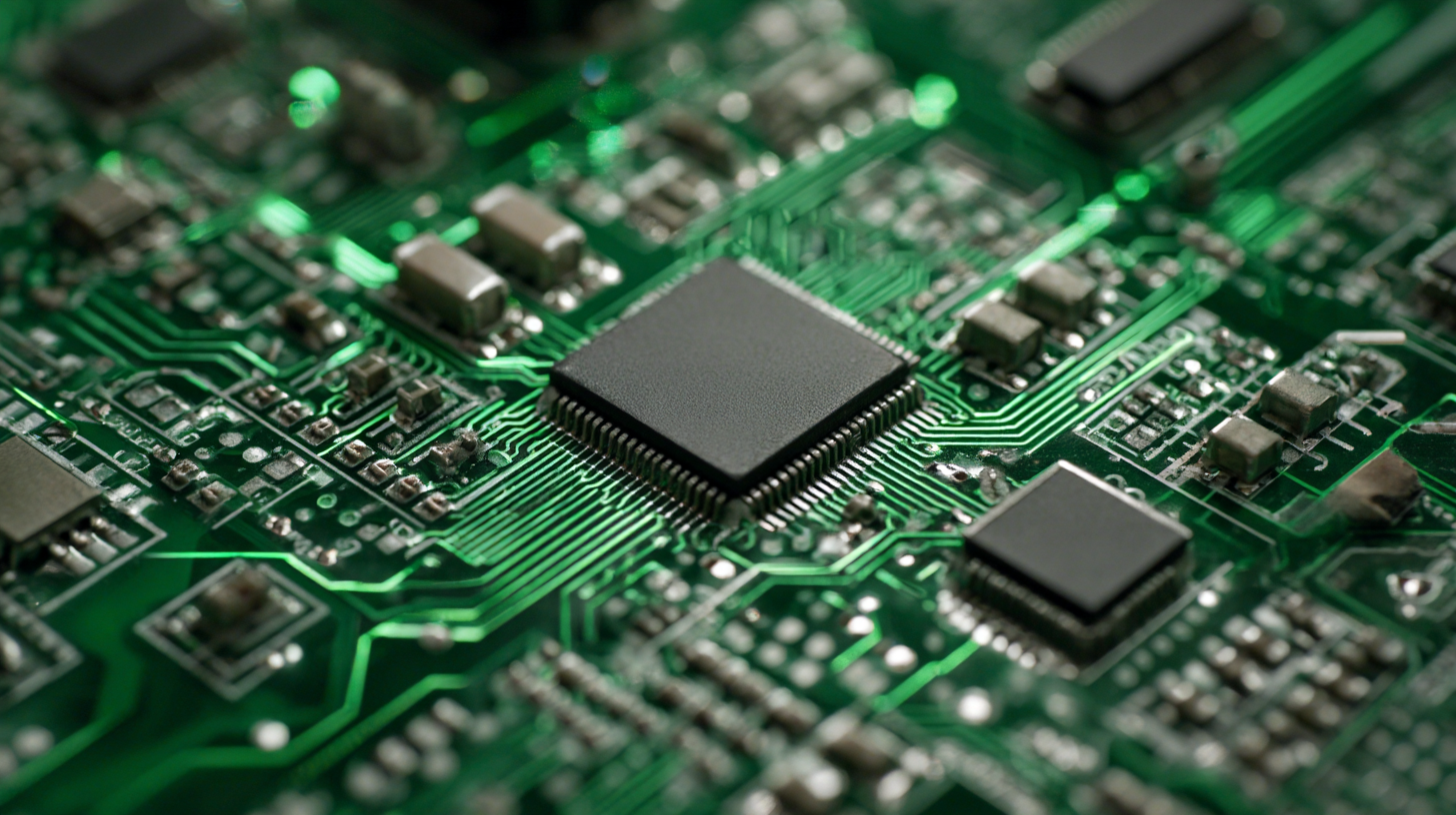
Understanding the basics of printed circuit board (PCB) design and functionality is crucial for anyone looking to delve into electronics. A PCB is essentially the backbone of any electronic device, providing a platform for components to interconnect and communicate. The layout of a PCB must be meticulously planned to ensure that signals can travel without interference, and that power is distributed evenly throughout the board. This means considering the size of the components, the paths of the traces, and the placement of vias to optimize performance.
**Tips:** Always start with a schematic diagram, as it serves as a blueprint for the physical board. Use software tools to simulate circuit behavior before moving on to the physical design. Also, pay attention to the design rules within your PCB design software to prevent manufacturing issues later on.
When it comes to the manufacturing aspect, understanding material selection is critical. The substrate material, usually FR-4, affects the board's performance, durability, and cost. Additionally, the finishing process, such as HASL or ENIG, can impact solderability and the long-term reliability of the PCB.
**Tips:** Keep your designs as simple as possible to reduce potential error sources. Consider using advanced fabrication techniques if your project involves high-frequency signals or requires intricate designs. By mastering these fundamentals, you can effectively move from concept to a functional PCB.
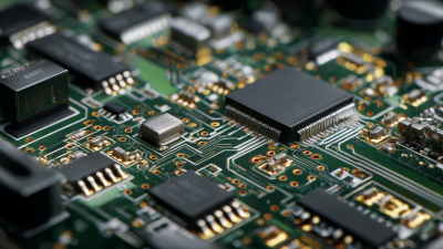
Choosing the Right Materials for High-Quality PCB Manufacturing
When it comes to designing and manufacturing a high-quality printed circuit board (PCB), the choice of materials is critical. Selecting the right substrate is the first step in ensuring the performance and longevity of the PCB. FR-4, a fiberglass epoxy laminate, is the most widely used material due to its excellent electrical properties and mechanical strength. However, for high-frequency applications, materials like Rogers or PTFE may be more suitable due to their superior dielectric properties.
Tips: Always consider the thermal properties of the materials you choose. Higher thermal conductivity is essential for applications that generate a lot of heat as it helps in heat dissipation, thereby maintaining circuit performance.
Another key aspect is the choice of copper thickness. Standard PCBs typically use 1 oz/ft², but for high-current applications, thicker copper layers (like 2 oz/ft² or more) can be beneficial. This helps reduce resistance and prevents overheating.
Tips: When selecting materials, consider not only the electrical and thermal aspects but also factors like cost and availability to ensure a balance between quality and budget.
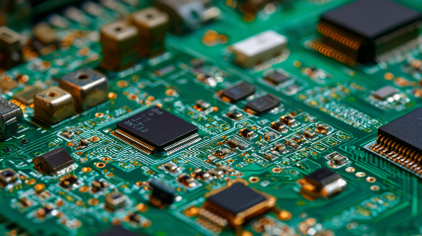
Step-by-Step Guide to Creating PCB Schematics and Layouts
 Creating high-quality printed circuit board (PCB) schematics and layouts is a critical step in the manufacturing process. According to a report by the IPC (Institute for Printed Circuits), over 70% of design errors occur during the schematic creation phase. This statistic underscores the importance of a meticulous approach to design. Start by selecting appropriate software tools, such as Altium Designer or KiCAD, which are widely recognized in the industry for their robust features that facilitate precise schematic creation. The initial design should emphasize component placement for optimal signal integrity while adhering to industry standards such as IPC-2221 for PCB design.
Once the schematic is finalized, transitioning to the PCB layout is the next essential phase. It is vital to define the board dimensions and layer stack-up carefully, as improper layout can lead to performance issues. A study published by Electronics Weekly indicates that a well-structured layout can reduce electromagnetic interference (EMI) by up to 30%. Effective routing techniques, including differential pairs and ground plane management, also play a significant role in achieving a high-quality PCB. By following these guidelines and continuously validating designs through simulations, developers can significantly enhance their chances of producing reliable and efficient PCBs that meet the fast-evolving demands of the electronics industry.
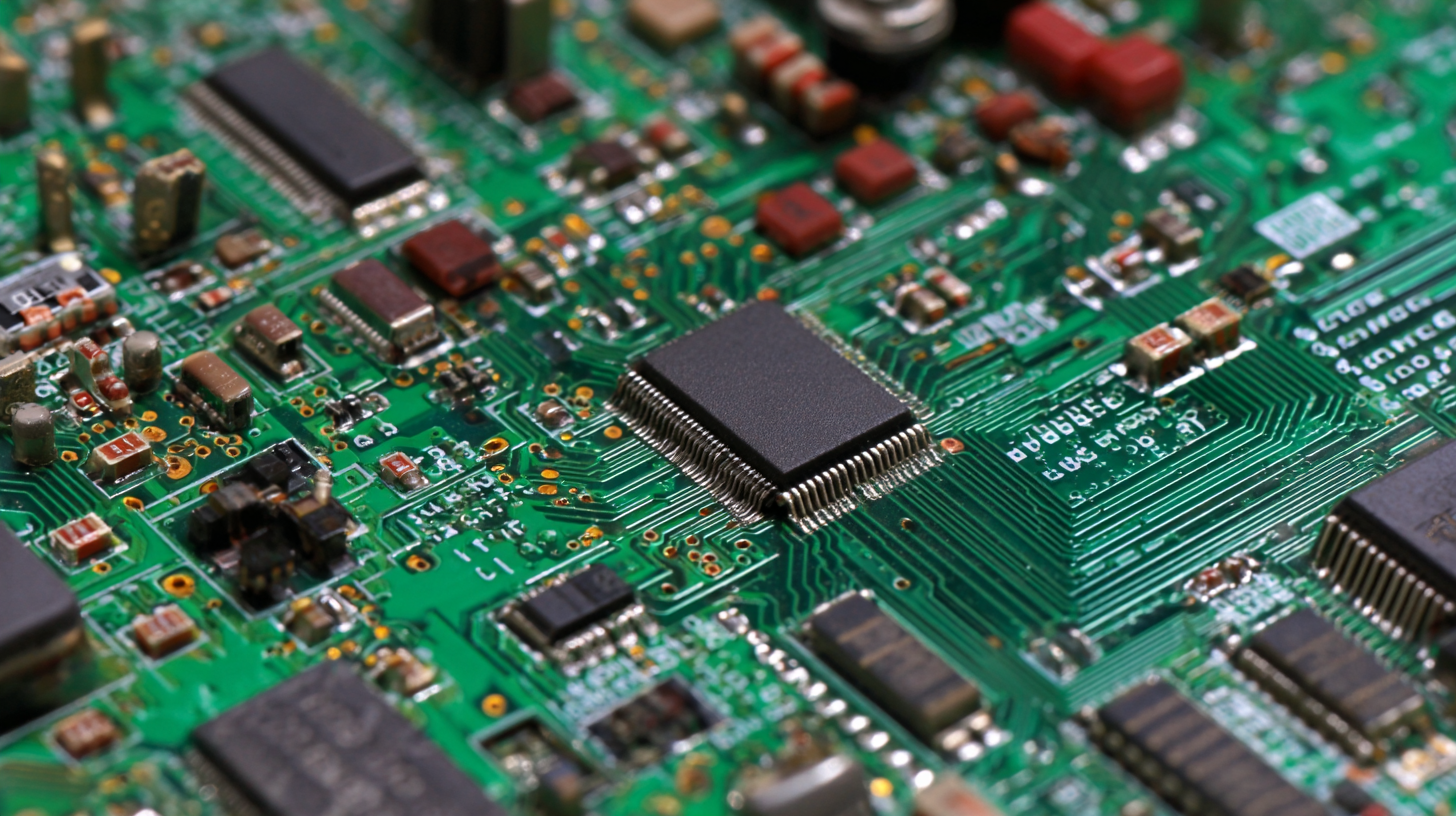
Techniques for Fabricating and Assembling Your Printed Circuit Board
In the realm of high-quality printed circuit board (PCB) design and manufacturing, recent advancements in fabrication techniques have paved the way for enhanced integration and performance, particularly in the development of lab-on-PCB technologies. The micro-total analysis system (µTAS), which emerged in the early 1990s, has significantly influenced the evolution of lab-on-a-chip devices, allowing for highly efficient chemical and biological analysis directly on a PCB. This innovation aligns with the industry’s increasing focus on miniaturization, which is crucial for wearable technologies that require electronics to conform seamlessly to the human body.
Furthermore, sustainable practices in PCB manufacturing are gaining traction, underscored by the findings that 3D printing could potentially lower total manufacturing costs and reduce CO2 emissions by as much as $593 billion. Techniques such as automated desktop wiring for micromodular systems have also emerged, facilitating the creation of intricate circuits with high resolution through submicron electrohydrodynamic jet printing. This progressive approach addresses significant challenges in wiring microscale modular components, ultimately enhancing the functionality and reliability of complex PCBs in a rapidly evolving technological landscape.
Testing and Quality Assurance Methods for Custom PCBs
When designing and manufacturing a high-quality printed circuit board (PCB), testing and quality assurance methods are crucial to ensure functionality and reliability. Various testing techniques can be employed throughout the production process to detect potential issues early on. Functional testing verifies the PCB performs its intended functions correctly, while in-circuit testing checks for manufacturing defects by measuring the electrical characteristics of individual components.
Tips: Always implement an automated optical inspection (AOI) system during the production phase. This system can quickly identify misalignments and soldering issues, significantly reducing the time needed for manual inspection. Furthermore, consider conducting thermal cycling tests to assess the PCB's performance under extreme temperature conditions, which helps uncover weaknesses that might not be evident under regular testing environments.
Another essential aspect of quality assurance is the use of robust design rules during the layout phase. By adhering to guidelines such as proper trace width for current capacity and adequate spacing to prevent shorts, you can improve both the durability and performance of your PCB. Implementing these practices not only enhances quality but also streamlines the manufacturing process, reducing the likelihood of costly rework or failures in the field.
Quality Assurance Metrics for Custom PCB Manufacturing