What is PCB Manufacturing and Assembly Process Explained for Beginners
The PCB manufacturing and assembly process is a critical aspect of the electronics industry, playing a pivotal role in the production of circuit boards that are essential for a wide range of devices. According to a report by MarketsandMarkets, the global printed circuit board market is projected to reach $82.51 billion by 2026, indicating the immense scale and significance of this industry. As technology continues to advance, understanding the intricacies of PCB manufacturing and assembly becomes paramount for both professionals and newcomers alike.
Expert insights enhance our understanding of this complex process. Dr. Emily Thompson, a renowned authority in the field of electronics manufacturing, states, "The evolving landscape of PCB manufacturing and assembly is characterized by innovation and efficiency, essential for meeting the demands of modern technology." Such insights underscore the importance of mastering the manufacturing techniques and assembly methods that contribute to the quality and reliability of electronic products.
In this article, we will explore the fundamental steps involved in PCB manufacturing and assembly, from initial design and material selection to the final assembly and testing processes. By demystifying these essential procedures, we aim to equip beginners with the knowledge needed to navigate the ever-expanding world of electronics manufacturing.
What is PCB Manufacturing and its Importance in Electronics Industry
PCB manufacturing plays a crucial role in the electronics industry, serving as the backbone for virtually all electronic devices. A printed circuit board (PCB) is responsible for mechanically supporting and electrically connecting various electronic components. As technology advances, PCBs have become increasingly sophisticated, enabling complex functions within smaller form factors, making them essential in everything from smartphones to industrial machinery.
The importance of PCB manufacturing lies in its ability to facilitate innovative designs while ensuring reliability and efficiency. High-quality PCBs can significantly enhance the performance of electronic products, contributing to longer lifespans and reduced failure rates. Moreover, as consumers demand more advanced technology, manufacturers rely on effective PCB assembly processes to meet these needs while managing production costs. The continual improvement of manufacturing methods not only streamlines production but also fosters advancements in technology, underscoring its vital role within the electronics sector.
Understanding PCB Manufacturing Process
This bar chart represents the different stages involved in the PCB manufacturing process along with their estimated duration in hours. The stages include Design, Material Selection, Fabrication, Assembly, Testing, and Packaging. This visualization helps to understand the time allocation for each step in the overall manufacturing process.
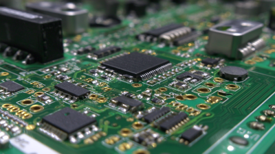
Understanding the Basic Components of a Printed Circuit Board
A printed circuit board (PCB) is a fundamental component in modern electronic devices, serving as the backbone that connects different electronic elements. At its core, a PCB comprises several essential components, including conductive pathways, insulating substrates, and electronic components such as resistors, capacitors, and integrated circuits. The substrate, typically made of fiberglass or other insulating materials, provides structural support and isolates the electrical pathways from one another. These pathways, usually copper traces, facilitate the flow of electricity between components, allowing the circuit to function effectively.
Understanding the basic components of a PCB is crucial for anyone interested in electronics. The electronic components mounted on the PCB can vary greatly depending on the device's purpose. For instance, resistors control the flow of current, while capacitors store and release electrical energy as needed. Integrated circuits, which can contain thousands of microscopic components, perform complex computations and processes. The arrangement and interaction of these parts on the PCB determine the device's overall functionality. Therefore, a solid grasp of these components and their roles is essential for anyone looking to design, manufacture, or troubleshoot PCBs in today’s technology-driven world.
Step-by-Step Guide to the PCB Design Process for Beginners
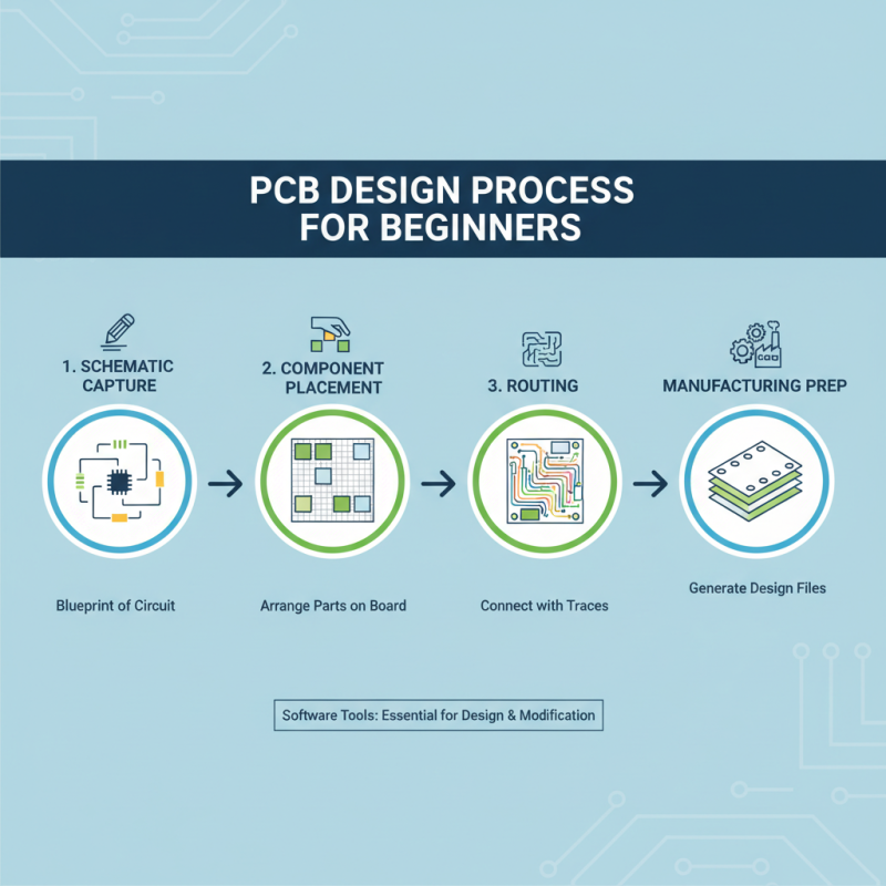
The PCB design process is a critical step in the manufacturing of printed circuit boards, particularly for beginners looking to create functional electronic devices. This process begins with the creation of a schematic diagram, which serves as a blueprint for the circuit's functionality. In this stage, designers specify components like resistors, capacitors, and integrated circuits, along with their interconnections. Software tools are often employed to facilitate this design, allowing for easy modifications and adjustments.
Once the schematic is finalized, the next step is converting it into a PCB layout. This involves arranging the components on a virtual board and routing the electrical connections between them. Designers must consider factors such as signal integrity and electromagnetic interference, ensuring that the layout supports efficient performance. Following the layout, designers proceed to generate the necessary design files, often referred to as Gerber files, which are essential for the PCB manufacturing process. This meticulous attention to detail in the design phase is vital for creating reliable and effective electronic products, making it an essential aspect for anyone venturing into PCB design.
The PCB Fabrication Process: From Material Selection to Etching
The PCB fabrication process is a critical step in electronics manufacturing, transforming raw materials into functioning printed circuit boards. First, material selection is crucial; typically, substrates like FR-4 or polyimide are chosen based on the required electrical properties and thermal stability. Once the material is selected, the design file is transferred to the fabrication stage, where patterns for the conductive pathways are etched onto the substrate using chemical processes. This process involves layering, imaging, and developing the patterns through photolithography, ensuring precision and accuracy.
Tips: Ensure that the design files are thoroughly checked for errors before sending them to fabrication. This helps minimize waste and reduces production time.
After etching the conductive layers, additional steps such as drilling vias and plating are performed. Vias enable electrical connections between different layers, and plating adds a layer of solder to the pads, preparing them for component assembly. During this phase, attention to detail is vital, as any imperfections can lead to a malfunctioning PCB.
Tips: Always utilize updated CAD software for accurate designs, and consider setting up a verification process with prototypes to avoid costly mistakes in the later assembly stages.
What is PCB Manufacturing and Assembly Process Explained for Beginners - The PCB Fabrication Process
| Process Step |
Description |
Materials Used |
Typical Duration |
| Material Selection |
Choosing the right substrate and conductive materials. |
FR-4, Copper, Aluminum |
1-2 days |
| Design |
Creating the PCB layout using CAD software. |
CAD software (e.g., Altium, Eagle) |
2-5 days |
| Photo-plotting |
Generating photomasks for exposing the PCB. |
Photoresist film |
1-2 days |
| Etching |
Removing excess copper to create the circuit pattern. |
Chemical etchants |
1 day |
| Drilling |
Creating holes for through-hole components and vias. |
Drill bits |
1 day |
| Plating |
Depositing metal onto the PCB for conductivity. |
Copper, Nickel, Gold |
2 days |
| Solder Mask Application |
Applying a protective layer to prevent solder bridging. |
Solder mask ink |
1 day |
| Component Placement |
Positioning electronic components on the PCB. |
PCB components |
1-2 days |
| Soldering |
Connecting components to the PCB through soldering. |
Solder wire or paste |
1 day |
| Testing |
Verifying the functionality of the assembled PCB. |
Testing equipment |
1-2 days |
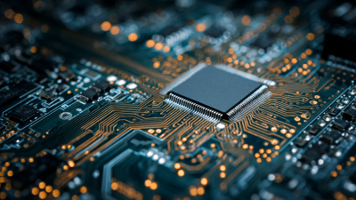
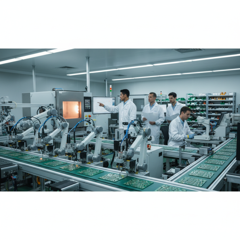
Overview of PCB Assembly: Soldering Techniques and Quality Control
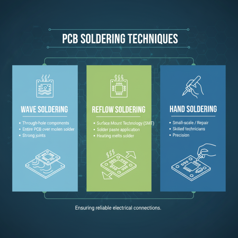
Soldering is a crucial technique in the PCB assembly process, ensuring that components are securely attached to the printed circuit board (PCB) for reliable electrical connections. There are several methods of soldering employed in PCB production, such as wave soldering, reflow soldering, and hand soldering. Wave soldering is primarily used for through-hole components, where the entire PCB is passed over a wave of molten solder, creating strong joints. Reflow soldering, on the other hand, is ideal for surface mount technology (SMT), where solder paste is initially applied to the pads, and then the assembly is heated to melt the solder and create connections. Hand soldering is typically reserved for small-scale production or repair jobs, requiring skilled technicians to ensure precision.
Quality control is an essential aspect of PCB assembly that focuses on ensuring reliability and performance in the final product. This involves thorough inspections and testing at various stages of the assembly process. Visual inspections are conducted to identify potential defects or misalignments, while automated optical inspection (AOI) systems provide more detailed analysis by detecting issues that may not be visible to the naked eye. In addition to inspections, functional testing methods are employed to evaluate how well the assembled board performs under operational conditions. By integrating robust quality control measures, manufacturers can minimize defects and ensure the longevity and efficiency of the assembled PCBs.