10 Smart Tips for Mastering PCB Circuit Design in the Digital Era
In the rapidly evolving landscape of electronics, mastering PCB circuit design has become more critical than ever. According to a report by Markets and Markets, the global printed circuit board market is projected to reach $90.28 billion by 2025, growing at a CAGR of 3.3% from 2020 to 2025. This growth is fueled by the increasing demand for advanced electronic devices and the Internet of Things (IoT), making efficient and innovative PCB circuit design essential for engineers and designers alike. In the digital era, where technology trends like miniaturization and high-frequency performance dominate, understanding the nuances of PCB circuit design can dramatically impact product reliability, speed of development, and manufacturing costs. This blog will explore ten smart tips to enhance your PCB circuit design skills, ensuring you stay ahead in this competitive industry.
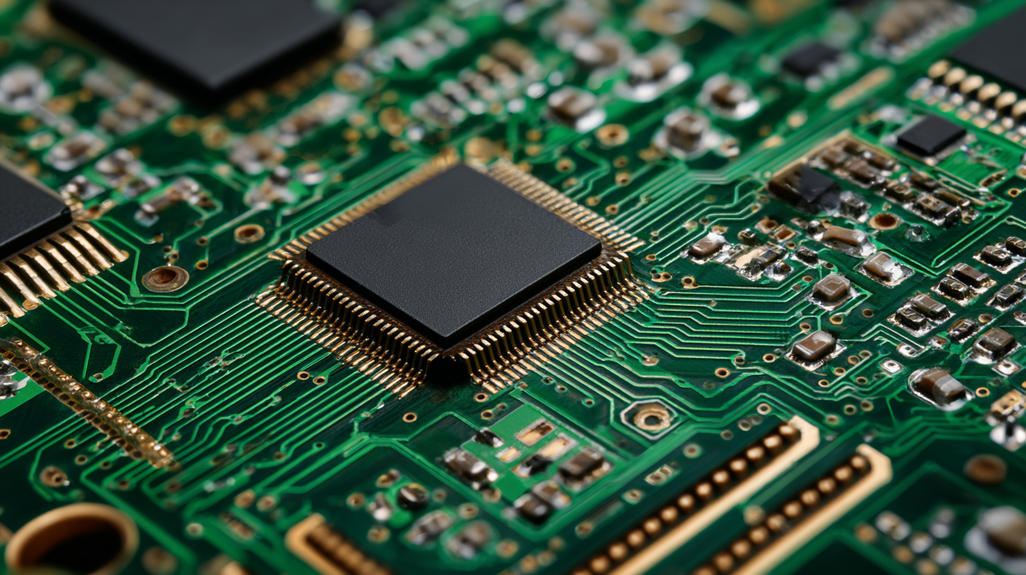
Understanding the Basics of PCB Design: Essential Principles You Need to Know
In the rapidly evolving field of electronics, mastering PCB circuit design has become essential for engineers and hobbyists alike. Understanding the fundamentals of PCB design can significantly impact the performance and efficiency of electronic devices. According to recent industry reports, the global PCB market is projected to reach $80 billion by 2027, driven by advancements in technology and increased demand for consumer electronics. This highlights the importance of staying updated with essential design principles, from selecting appropriate materials to ensuring proper signal integrity.
One crucial aspect of PCB design is the consideration of layer stacking and routing strategies. Effective layer management is key to minimizing electromagnetic interference (EMI) and maximizing thermal performance. Studies suggest that optimizing layer architecture can reduce signal degradation by up to 30%, underscoring the importance of strategic planning in circuit layout. Additionally, embracing modern tools and software, such as those recommended in the latest evaluations, can enhance productivity and accuracy. With educational resources now more accessible, including free courses offered by various platforms, aspiring designers are well-equipped to tackle the challenges of PCB design in today’s digital landscape.
10 Smart Tips for Mastering PCB Circuit Design in the Digital Era - Understanding the Basics of PCB Design: Essential Principles You Need to Know
| Tip |
Description |
Benefits |
| Understand Your Requirements |
Clearly define the project specifications before starting design. |
Avoids redesigns and saves time. |
| Use EDA Software |
Utilize Electronic Design Automation tools for efficient layout and simulation. |
Enhances accuracy and speeds up the design process. |
| Design for Manufacturability |
Consider production capabilities and limits during design. |
Reduces production costs and improves yield. |
| Plan Your Layer Stack |
Optimize the number of layers based on your circuit complexity. |
Minimizes size and weight while maintaining performance. |
| Pay Attention to the Layout |
Organize components logically, keeping signal paths short. |
Improves signal integrity and reduces interference. |
| Incorporate Simulation Tools |
Use simulation for thermal, signal integrity, and timing analysis. |
Proactively identifies potential issues before production. |
| Optimize Component Placement |
Place components to minimize trace lengths and improve airflow. |
Enhances performance and thermal management. |
| Use Standard Components |
Select widely available and cost-effective components. |
Ensures ease of sourcing and cost efficiency. |
| Review and Revise |
Conduct thorough reviews with peers or mentors. |
Catches mistakes and enhances overall design quality. |
Utilizing Advanced CAD Tools for Enhanced Circuit Design Efficiency
In the realm of PCB circuit design, the advent of advanced CAD tools has revolutionized the way engineers approach their projects. These tools not only streamline the design process but also enhance the accuracy and efficiency of circuit layouts. With features like real-time simulation and automated error checking, designers can quickly identify potential issues before they become costly mistakes. The integration of sophisticated algorithms allows for optimized routing and placement, ensuring that the final product meets both performance and reliability standards.

Moreover, advanced CAD software often includes user-friendly interfaces and customizable libraries, which cater to the specific needs of modern engineers. This flexibility enables designers to easily adapt their designs to incorporate emerging technologies, thereby accelerating the development cycle. Collaboration tools integrated within these CAD platforms further facilitate communication among team members, allowing for seamless project management and quicker iterations. By leveraging these powerful resources, PCB designers can not only meet the demands of the digital era but also push the boundaries of innovation in circuit design.
Incorporating Design for Manufacturability (DFM) in Your PCB Projects
Incorporating Design for Manufacturability (DFM) into PCB projects is essential for ensuring high-quality outcomes in today's rapidly evolving digital landscape. DFM principles emphasize optimizing designs to simplify manufacturing processes, reduce costs, and enhance product performance. As product miniaturization and complexity increase, attention to DFM becomes even more critical. Research shows that integrating DFM early in the design phase can reduce production costs by up to $20% and increase the speed of bringing products to market.
Tip 1: Leverage advanced design tools that include DFM capabilities, such as the latest additions to PCB design suites. These tools help identify potential manufacturing issues before they arise, allowing designers to make necessary adjustments promptly. For example, the recently launched DFM tools have been proven effective in addressing common design pitfalls that can lead to costly revisions during production.
Tip 2: Collaborate closely with manufacturing teams during the design phase. Engaging with manufacturers early in the process can provide insights into their capabilities and limitations, helping you to design with manufacturability in mind. Statistics indicate that projects benefiting from cross-functional collaboration enjoy a 30% reduction in design iterations, contributing to a more efficient development cycle and enhanced product reliability.
Employing Simulation Techniques to Predict Circuit Performance Before Production
In the digital era, the complexities of PCB circuit design necessitate advanced simulation techniques to predict circuit performance before production. According to a report by ResearchAndMarkets, the PCB simulation market is expected to reach $1.1 billion by 2027, reflecting a growing reliance on simulation tools to reduce the risk of design flaws and minimize costly revisions. By leveraging simulation software, engineers can analyze critical parameters such as signal integrity, thermal behavior, and electromagnetic interference, enabling them to optimize designs in a virtual environment before advancing to prototypes.
Utilizing tools like finite element analysis (FEA) and circuit simulation, designers can gain insights into how their circuits will perform under various operating conditions. A study published by IPC demonstrated that early-stage simulation can reduce prototype development time by up to 30%, underscoring the efficiency gained by modeling designs digitally. By harnessing these techniques, PCB designers not only enhance product reliability but also align with rapid market demands, which require faster turnaround times and innovation to maintain a competitive edge.
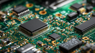
10 Smart Tips for Mastering PCB Circuit Design in the Digital Era
This bar chart represents the predicted circuit performance metrics using simulation techniques applied in PCB design. The data showcases different simulation methods' effectiveness in improving the overall design outcomes.
Staying Current: Navigating Emerging Trends and Technologies in PCB Design
In today's fast-evolving electronics landscape, mastering PCB circuit design demands an awareness of emerging trends and technologies. The continued rise of wearable devices, especially in healthcare applications like glucose monitoring, is transforming the industry. According to recent reports, the global wearable device market is projected to exceed $62 billion by 2025, highlighting the importance of integrating advanced sensing technologies into PCB designs. Such advancements require designers to incorporate miniaturization and consider materials that enhance performance while reducing footprint.
To stay competitive, PCB designers must adopt strategic approaches to leverage current industry trends. One critical tip is to embrace AI and IoT innovations; they significantly enhance circuit efficiency and enable smarter functionality in devices. Another essential strategy involves understanding the environmental impact of PCBs, particularly related to e-waste management—a pressing issue as urban mining and recyclability become focal points in sustainable design practices. By focusing on these trends and incorporating them into your designs, you position your projects to thrive in a rapidly changing market.